- Some electric vehicles Tesla Model S are equipped with more capacious batteries - AMD counts on the long life of the 7-nm process technology - The next generation of Microsoft HoloLens will receive an advanced specialized processor - Samsung is determined to narrow the gap with TSMC in the contract manufacturing market -
![]()
|
xtreview is your : Video card - cpu - memory - Hard drive - power supply unit source |
|
|
|
|
||

|
POSTER: computer news || SOME ELECTRIC VEHICLES TESLA MODEL S ARE EQUIPPED WITH MORE CAPACIOUS BATTERIES |
DATE:2017-07-25 |
|
As noted profile resources, with the advent of Tesla's younger model 3 in the range of electric vehicles, the Tesla Model S traction battery can be reformed - in any case, the initial version with a battery of 75 kWh and a single-axis drive will be removed by the end of the year. Not so long ago Tesla Model S was offered in the version with a battery capacity of 60 kW � h, which could be unlocked . Electrek website notes that among the fresh samples of Tesla Model S and Model X delivered to Norway there were at least six pieces equipped with a traction battery with a declared capacity of 85 kWh. Note that earlier this modification of the Tesla Model S was offered officially, until it gave way to the option with a battery capacity of 90 kWh (already discontinued), but in this case we are talking about electric vehicles Tesla Model S 75, Model S 75D and Model X 75D. In fact, the actual capacity of their battery is higher than the one declared at the time of purchase. 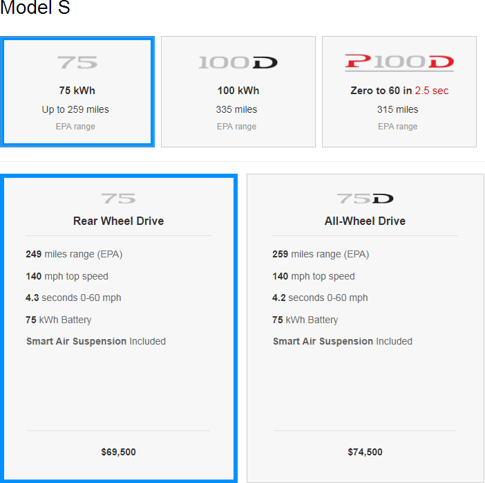 At the same time, there are no proposals on the Tesla website for activating an additional 10 kWh,. 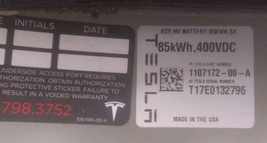 It can be assumed that after entering the market of Tesla Model 3, whose bundle of traction battery capacity has not yet been announced, the company will raise the "lower battery capacity bar" for the Tesla Model S and Model X, and options with a 75 kWh battery will be abolished Completely. Select Rating :Some electric vehicles Tesla Model S are equipped with more capacious batteries |
Add Comment ( 1 ) SOME ELECTRIC VEHICLES TESLA MODEL S ARE EQUIPPED WITH MORE CAPACIOUS BATTERIES |
|
|
|

|
POSTER: computer news || AMD COUNTS ON THE LONG LIFE OF THE 7-NM PROCESS TECHNOLOGY |
DATE:2017-07-25 |
|
AMD company can be considered one of the few who have already tasted the 7-nm process technology. Processors Zen 2 are designed taking into account the 7-nm production technology, which makes them a new level of requirements. This is a serious challenge, AMD's chief technologist Mark Pepermaster (Mark Papermaster) admitted in an interview to the Internet resource EE Times. The company had to literally double its efforts and resources aimed at designing solutions with the norms of 7 nm. And the technical process with these production standards will have a very long life, approximately, like in the 28-nm process technology. Processors Zen 3 will also use a 7-nm process technology. Go from 14/16 nm to 7 nm - this is how to jump in time from metal compounds in chips to copper connections. This is a small revolution. But this made it necessary to revise almost all the stages of design. Transistors have to be connected "in a different way", also another construction of blocks is required. In addition, the complexity of the work has increased many times because of the need to use four photomasks instead of two for the production of critical layers. The reduction in the cost of production can be expected no earlier than after 2019, when EUV-scanners start operating at the manufacturing enterprises. Scanners with a wavelength of 13.5 nm by GlobalFoundries and TSMC (AMD's production partners) are planning to launch into commercial work in 2019. In the first year, hardly any breakthrough is expected, but in 2020-2021 the effect of switching to EUV lithography can be felt in full growth. Another alternative to reduce the cost of production of complex solutions should be the method of inexpensive packaging of several chips in a single case. In the future, the industry seeks vertical (stack) structures using end-to-end metal connections such as TSVs. Placement on one substrate of the processor (GPU) and memory of the HBM type is considered expensive at cost. This is the so-called 2.5 D technology. The alternative is 2.1 D packaging, when the substrate and crystals are filled with sealant, turning into one housing - not yet suitable for the production of computer central and graphics processors. Therefore, AMD developers urge manufacturers to adapt this type of packaging to processors and see in it the possibility to continue the work of Moore's law. Fortunately for AMD, a similar type of packaging is the Integrated Fan Out Wafer-level Package (InFO-WLP) - practiced by TSMC. For example, the latest Apple processors are packed with this method. There is a non-zero probability that TSMC will be able to adapt the InFO-WLP packaging for the release of AMD solutions. Finally, AMD encourages developers of software tools for designing chips to make maximum efforts to optimize packages for designers. According to AMD, software for design does not fully use the parallelism in applications. This is all the more offensive, because AMD has prepared 32-core processors with support for 64 threads each. The complexity of projects is growing at a horrendous pace, and the tools are not improving as quickly as one would like. Select Rating :AMD counts on the long life of the 7-nm process technology |
Add Comment ( 1 ) AMD COUNTS ON THE LONG LIFE OF THE 7-NM PROCESS TECHNOLOGY |
|
|
|

|
POSTER: computer news || THE NEXT GENERATION OF MICROSOFT HOLOLENS WILL RECEIVE AN ADVANCED SPECIALIZED PROCESSOR |
DATE:2017-07-25 |
|
Looking for a place in the new world, Intel Corporation, if necessary, can always say that its Cherry Trail Atom processor was used in the helmet of the augmented reality of Microsoft HoloLens of the first generation, along with a specialized "HP holographic processor" of Microsoft's own development. From the periodic statements of software giant representatives , it becomes clear that when creating such devices in the future, Microsoft would like to rely on the use of deep neural networks and artificial intelligence technology, without abandoning the processing of basic operations by the forces of "airborne equipment." In this context, it is interesting to hear a new revelation of Microsoft representatives from the pages of the corporate blog . Employees of the corporation responsible for the development of the HoloLens successor claim that the second generation device will receive a fundamentally new processor capable of efficiently working with deep neural networks - for this, HPU will have a special coprocessor. This HPU is currently under development, but Microsoft already has working samples. Select Rating : The next generation of Microsoft HoloLens will receive an advanced specialized processor |
Add Comment ( 1 ) THE NEXT GENERATION OF MICROSOFT HOLOLENS WILL RECEIVE AN ADVANCED SPECIALIZED PROCESSOR |
|
|
|

|
POSTER: computer news || SAMSUNG IS DETERMINED TO NARROW THE GAP WITH TSMC IN THE CONTRACT MANUFACTURING MARKET |
DATE:2017-07-25 |
|
The head of the profile division Samsung admitted in an interview with Reuters , the South Korean giant is ready to challenge competitors in the services market for contract manufacturing of semiconductor products, and to take the second position, second only to the recognized leader of TSMC. The latter controls 50.6% of the market, and to achieve the goal Samsung is ready in the next five years to increase its market share from 7.9% to 25%. Behind will remain not only UMC, but also GlobalFoundries. In May this year, the "contract" production of Samsung was allocated to an independent structural unit, and further expansion is quite a logical step. Relying on the market for Samsung memory chips is already tired, because it is quite changeable, and now the company is ready to attract new customers of various sizes, offering them services for the contract production of various semiconductor products. Samsung customers include Qualcomm, NVIDIA and NXP Semiconductors. The Korean company hopes to introduce a flexible production model, based on the use of lines for memory chips production. Already in the second half of next year, Samsung intends to begin production with the use of so-called EUV-lithography. The company competes with TSMC in terms of the development of this technology, designed to extend the so-called "Moore's Law". New technologies require significant investment, and expanding the customer base is a logical way to accelerate the return of funds. By the way, the rise in memory prices could well allow Samsung to bypass the Intel Corporation, which is considered to be the largest semiconductor manufacturer (in terms of money), in terms of revenues this year. According to representatives of Samsung, only "capable to surprise customers with technology" will allow the company to entice customers from competitors. Select Rating : Samsung is determined to narrow the gap with TSMC in the contract manufacturing market |
Add Comment ( 1 ) SAMSUNG IS DETERMINED TO NARROW THE GAP WITH TSMC IN THE CONTRACT MANUFACTURING MARKET |
|
|
|
|
xtreview is your : Video card - cpu - memory - Hard drive - power supply unit source |
|
|
|
|
||
![]()
To figure out your best laptops .Welcome to XTreview.com. Here u can find a complete computer hardware guide and laptop rating .More than 500 reviews of modern PC to understand the basic architecture


7600gt review
7600gt is the middle card range.
We already benchmarked this video card and found that ...
 geforce 8800gtx and 8800gts Xtreview software download Section AMD TURION 64 X2 REVIEW INTEL PENTIUM D 920 , INTEL PENTIUM D 930 6800XT REVIEW computer hardware REVIEW INTEL CONROE CORE DUO 2 REVIEW VS AMD AM2 INTEL PENTIUM D 805 INTEL D805 Free desktop wallpaper online fighting game Xtreview price comparison center
- 233 - E8600 vs q9400 which is better dual or quad core
Date : 2008-11-21
- 216 - Intel core 2 duo e6550 review and overclocking
Date : 2007-08-03
- 212 - Intel core 2 extreme qx6850 and core 2 duo e6850 review benchmark and overclocking
Date : 2007-07-16
- 205 - Amd athlon x2 be review , overclocking and energy consumption test
Date : 2007-06-05
- 229 - Radeon hd 4670 vs geforce 9500 gt vs geforce 9800 gt vs hd 4850 overclock benchmark and review
Date : 2008-10-10
- 228 - Crossfire hd 4870 x2 vs crossfire hd 4870 review and benchamrk
Date : 2008-09-26
- 226 - Amd radeon hd 4870 x2 2x1gb xtreview exclusive review
Date : 2008-07-14
- 220 - Nvidia 9600 gt review and benchmark
Date : 2008-02-27
- 131 - 500 to 750 gig hdd round up : maxtor wd seagate hitachi
Date : 2006-07-10
- 65 - Raptor x hdd western digital review overview : pcmark - benchmark - test
Date : 2006-05-06
- 193 - Asus s6fm-1p039e vs sony vaio vgn-g11xn/b vs lenovo 3000 v100 review and benchmark
Date : 2007-05-11
- 172 - Apple imac 20 inch - intel core 2 duo review
Date : 2007-01-26
- 102 - Toshiba tecra a6-s513 review notebook performance benchmark
Date : 2006-06-09
- 101 - Sony vgn-fj1sr review notebook performance benchmark
Date : 2006-06-09
SnagIt v.9.1.22009-04-24
Daemon Tool v.4.30.42009-04-24
WinSCP v.4.1.92009-04-24
Vista Codec Package v.5.2.02009-04-24
Vista Codec x64 Components v.1.8.12009-04-24
Anti-keylogger v.9.2.12009-04-24
Portable Firefox v.3.0.92009-04-24
AVG Internet Security v.8.5.322a14952009-04-24
Universal Viewver v.4.0.02009-04-24
Wise Disk Cleaner v.4.242009-04-24
FeedDemon v.3.0.0.16 Beta2009-04-24
SiSoft Sandra 2009 SP2 (2009.5.15.96)2009-04-24
Atheros AR5xxx Driver v.7.7.0.2332009-04-24
Bios update for 24 April2009-04-24
AIMP Classic v.2.60 Build 466 Beta 12009-04-23
SpeedFan v.4.382009-04-23
- The new version of GPU-Z finally kills the belief in the miracle of Vega transformation
- The motherboard manufacturer confirms the characteristics of the processors Coffee Lake
- We are looking for copper coolers on NVIDIA Volta computing accelerators
- Unofficially about Intels plans to release 300-series chipset
- The Japanese representation of AMD offered monetary compensation to the first buyers of Ryzen Threadripper
- This year will not be released more than 45 million motherboards
- TSMC denies the presentation of charges from the antimonopoly authorities
- Radeon RX Vega 64 at frequencies 1802-1000 MHz updated the record GPUPI 1B
- AMD itself would like to believe that mobile processors Ryzen have already been released
- AMD Vega 20 will find application in accelerating computations
- Pre-orders for new iPhone start next week
- Radeon RX Vega 57, 58 and 59: the wonders of transformation
- ASML starts commercial delivery of EUV-scanners
- The older Skylake processors with a free multiplier are removed from production
- Meizu will release Android-smartphone based on Helio P40
- AMD Bristol Ridge processors are also available in American retail
- The fate of Toshiba Memory can be solved to the next environment
- duo GeForce GTX 1080 Ti in GPUPI 1B at frequencies of 2480-10320 MHz
- New Kentsfield overclocking record up to 5204 MHz
- Lenovo released Android-smartphone K8
Affiliates


computer news computer parts review OLD Forum Downloads New Forum Login Join Articles terms Hardware blog Sitemap myspace proxy Get Freebies